
New EDA Challenges and Tool Iterations Driven by Advanced Packaging
Advanced packaging has changed the semiconductor design flow in a way that feels subtle at first and then suddenly unavoidable. What used to be the back end of the line—package selection, assembly, and test—has become a co-equal design domain alongside logic, memory, and interconnect. As heterogeneous integration moves from a niche practice to the default architecture for high-end AI, HPC, networking, and mobile systems, EDA tools are being pushed far beyond their traditional boundaries.
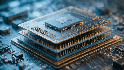
This shift is not just about adding a few package viewers or bump maps to an existing flow. It is forcing major iterations in system partitioning, co-design, thermal analysis, power integrity, signal integrity, mechanical stress modeling, and even data management. In other words, advanced packaging is making EDA grow up. The tools now need to understand not only transistors and wires on a die, but how multiple dies interact inside a package, how the package interacts with the board, and how all of that behaves under real operating conditions.
Why Packaging Became an EDA Problem
For a long time, the chip and the package were treated as separate worlds. The chip team optimized the SoC. The package team picked from a small set of standard options. The board team took whatever came out the other side. That division worked when packages were relatively simple and the chip itself carried most of the system complexity.
Advanced packaging breaks that model. Today’s systems often include:
- Multiple chiplets on a 2.5D interposer.
- HBM stacks sitting inches away from compute in bandwidth terms but microns away physically.
- 3D IC structures with vertically stacked logic or memory dies.
- Fan-out and system-in-package modules that integrate logic, RF, power, and passives.
Once those architectures enter the picture, package choices directly affect timing, bandwidth, thermal behavior, reliability, yield, and cost. You can’t finalize the die without understanding the package, and you can’t finalize the package without understanding the die. That circular dependency is exactly why EDA has become one of the main battlegrounds in heterogeneous integration.
The End of Silos

The biggest conceptual change is the collapse of the old silos between chip design, package design, and board design. In an advanced packaging world, these teams must work from a shared system model. A design error in one layer can undo months of work in another.
For example, a chiplet may meet all electrical targets in isolation, but once it is placed on an interposer next to HBM, the combined power delivery network may cause voltage droop. Or a package may look mechanically sound, but a poorly placed die can create a thermal hotspot that forces the entire system to throttle. Or a beautiful timing closure on the die may be ruined by package routing constraints that add too much latency.
EDA tools are therefore being asked to do something they were not originally built for: model the package and the chip as a single coherent system. That sounds straightforward in principle, but in practice it means integrating data structures, analysis engines, and signoff methodologies that were once separate product families.
Partitioning Becomes a First-Class Design Step
In monolithic design, partitioning was mostly an internal floorplanning issue. In chiplet-based systems, partitioning becomes a strategic decision with packaging implications. Which functions belong on the leading-edge node? Which can move to mature silicon? Which blocks need to be physically close? Which links are bandwidth-critical? Which dies are thermally sensitive?
EDA tools must help answer these questions early, not late. That requires new forms of architecture exploration and package-aware design-space search. Designers now need to evaluate:
- Whether to split a design across multiple chiplets or keep it monolithic.
- How to balance die size, yield, and package interconnect complexity.
- How many HBM stacks the package can support before routing and thermal limits become painful.
- Whether 2.5D, 3D, fan-out, or hybrid bonding is the right integration path.
This is not a minor tooling upgrade. It means EDA platforms must support higher-level architectural modeling, sometimes before a RTL design is even fully defined. That makes early exploration more important—and more difficult—than it used to be.
New Workflow Requirements

Advanced packaging forces EDA workflows to become more iterative and more interconnected. A typical flow might now include package-aware floorplanning, multi-die placement, die-to-die interface planning, thermal simulation, substrate routing, power network analysis, and reliability checks, all before final tape-out or package release.
That creates several new requirements:
- Unified databases. Data must move cleanly between chip, package, and board tools without translation errors or loss of fidelity.
- Fast iteration. Because packaging decisions are made earlier and revisited often, simulation and optimization loops need to be much faster.
- Cross-domain visibility. A change in die placement should immediately show up in thermal, timing, and PDN analysis.
- Version coherence. Multiple teams need to work on one system without breaking each other’s assumptions.
The old “throw it over the wall” flow is now mostly a liability. The winners in advanced packaging will be the teams that can iterate quickly across die, package, and board, while keeping design intent intact.
Thermal and Mechanical Modeling Are No Longer Optional
One of the most obvious EDA challenges driven by advanced packaging is thermal management. As more functionality is packed into a smaller volume, heat density goes up and thermal paths become more complicated. A chiplet that behaves nicely on a spreadsheet may become a disaster when stacked above another hot die or placed near an HBM tower.
EDA tools therefore need tighter thermal integration, including:
- Steady-state and transient thermal simulation.
- Coupled electro-thermal analysis.
- Package-level hotspot prediction.
- Thermal-aware placement and routing guidance.
Mechanical modeling is just as important. Warpage, stress, and coefficient-of-thermal-expansion mismatch can all affect yield and long-term reliability. A package that is electrically elegant but mechanically fragile is not a successful design. As a result, EDA vendors are adding more sophisticated stress analysis, chiplet stack modeling, and package deformation simulation into the design flow.
The interesting part is that these analyses are no longer isolated signoff steps. They are being pulled upstream into early planning because package geometry now influences the entire product architecture.
Signal Integrity at Package Scale
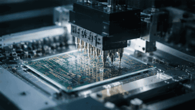
High-speed die-to-die communication is one of the reasons advanced packaging exists in the first place. But that same benefit creates a new set of EDA challenges. As links move from board-level traces to fine-pitch package interconnects, the margin for error shrinks. Parasitics, crosstalk, impedance discontinuities, and return-path issues all become more sensitive.
This means tools have to model the package with much greater fidelity than before. Designers need to see:
- Detailed interconnect parasitics across micro-bumps, RDLs, interposers, and substrate layers.
- Cross-coupling between adjacent chiplet interfaces.
- The effect of power delivery noise on high-speed links.
- How package topology changes impact eye diagrams and latency.
At advanced packaging densities, even small changes in die placement or routing can alter the behavior of high-speed channels. That means post-layout simulation has to become more iterative and more package-aware. Signal integrity is no longer just a chip or board problem; it is an ecosystem problem.
EDA for Heterogeneous Integration
Heterogeneous integration adds another level of complexity because it mixes technologies that were never meant to live together in the same package. One die may use an advanced logic node. Another may use mature silicon for I/O or analog. A third may be a memory stack. A fourth could be a chiplet from a third-party vendor.
EDA tools now need to support heterogeneous modeling across process, electrical, thermal, and mechanical domains. That includes:
- Different design rules for each die.
- Varied interface standards between chiplets.
- Different voltage domains and power sequencing requirements.
- Different reliability assumptions across nodes and materials.
In this environment, the package becomes the integration fabric. EDA must help architects decide how to partition functions across dissimilar dies and how to connect them through the package in a way that preserves performance and manageability. That is a very different problem from traditional SoC design, and it requires new abstractions.
Tool Iterations Are Happening Fast
One of the most interesting aspects of the current moment is how quickly EDA tools are evolving. A few years ago, many package-related features were limited to visualization or late-stage analysis. Now they are being integrated into exploratory design and even architectural planning.
Several trends stand out:
- Package-aware floorplanning is being added earlier in design cycles.
- Multi-die system simulation is becoming more automated.
- Constraint management across chip, package, and board is getting tighter.
- AI-assisted optimization is being used to explore placement and routing trade-offs.
This is not just incremental polish. It reflects a real change in how tools are expected to behave. EDA vendors must now support a “design everything together” mindset, where the package is treated as part of the system architecture, not as an external constraint.
The Pressure on Standards and Data Exchange
Whenever tools and workflows become more interconnected, data exchange becomes a critical issue. Advanced packaging makes that especially hard because the chip, package, and board worlds often use different file formats, naming conventions, and abstraction levels.
For example, a chip designer may think in terms of pins, nets, timing arcs, and power domains, while a package designer thinks in terms of dies, bumps, RDL layers, and substrate routing. The board team may care about connectors, rails, cooling, and mechanical keepouts. EDA tools need to move all of that data around cleanly and preserve the meaning of the design.
This has pushed the industry toward better standards and more robust translation layers. But the problem is not fully solved. In many projects, a lot of time is still spent reconciling naming mismatches, coordinate systems, and layer maps. That is one reason advanced packaging still feels difficult: the tools are improving, but the underlying ecosystem has not fully standardized around the new reality.
AI Is Changing EDA Too
It would be odd to talk about advanced packaging without noticing the irony that AI is both the driver of packaging demand and a tool for solving packaging problems. EDA vendors are increasingly using machine learning and optimization algorithms to help with:
- Thermal hotspot prediction.
- Package floorplan exploration.
- Yield and reliability estimation.
- Routing and placement optimization across multiple dies.
AI-assisted EDA is especially promising in advanced packaging because the design space is enormous. There are too many possible chiplet placements, die sizes, interconnect patterns, and thermal solutions for manual exploration alone. AI can help rank options, identify hidden trade-offs, and accelerate design iterations.
That said, AI does not replace engineering judgment. It works best as a guide, especially when combined with physics-based models. In advanced packaging, that hybrid approach is probably the right one: use AI to search, and use analysis to verify.
What Designers Need to Learn
The packaging revolution is also a skills revolution. Chip designers can no longer afford to ignore package effects, and package engineers need to understand enough system architecture to make meaningful trade-offs. EDA tools are only part of the answer; the human workflow must evolve too.
Future-facing teams are increasingly learning:
- How to think in terms of die-to-die interfaces instead of only on-die interconnect.
- How to evaluate thermal and mechanical constraints alongside timing closure.
- How to collaborate across chip, package, and board domains without creating bottlenecks.
- How to use early-stage simulation to reduce late-stage surprises.
This broader skill set is becoming essential because advanced packaging demands systems thinking. The best engineers in this space are often the ones who can see the whole stack at once.
Where the Next Iterations Are Heading
The next generation of EDA tools for advanced packaging will likely focus on three big themes: speed, integration, and intelligence. Speed means faster simulation and optimization. Integration means a more seamless flow across chip, package, and board. Intelligence means more automation, more predictive modeling, and more package-aware design guidance.
We can also expect tools to become more specialized for particular advanced packaging technologies:
- 2.5D interposer-aware tools for AI accelerators and HBM systems.
- 3D stacking workflows for hybrid bonding and vertically integrated dies.
- Fan-out and panel-level packaging tools for mobile, automotive, and consumer devices.
As heterogeneous integration continues to expand, EDA will keep iterating toward a world where package-level design is not an extension of chip design, but a full discipline of its own.
Conclusion
Advanced packaging has done something remarkable to EDA: it has made the package impossible to ignore. What was once a downstream implementation detail is now a central part of architecture, performance, cost, and reliability. That has forced tools to evolve quickly, and the evolution is still underway.
The new EDA challenge is not just to model more complexity. It is to help designers manage complexity intelligently across heterogeneous systems. The tools must support faster iteration, better co-design, and deeper analysis across thermal, electrical, and mechanical domains. As advanced packaging continues to expand, the companies that build the best EDA workflows will help define not just how chips are designed, but how entire computing systems are assembled from many different pieces of silicon.
You May Like

Narrowing Spread Between NAND Spot and Contract Prices in 2026 – A Signal
By 2026, one of the most watched metrics in the NAND flash market has started to shift in a subtle but meaningful way: the spread between spot prices and long‑term contract prices is narrowing. For casual observers, this may look like just another incremental change in a notoriously volatile industry. For memory makers, module houses, device OEMs, and data center buyers, however, a tightening gap between spot and contract prices is a signal—a reflection of evolving supply–demand balance, risk perceptions, and strategic behavior on both sides of the market.

Price Divergence Trading Strategies Between NAND Flash and DRAM ETFs
NAND flash and DRAM sit at the core of AI storage and computing power. Both are memory, but they are not the same business. DRAM is main memory—fast, volatile, and central to high‑bandwidth workloads like AI training and inference. NAND is non‑volatile storage—slower than DRAM, but crucial to persistent data and large‑scale object storage. The cycles that drive their pricing and margins overlap, yet they often diverge. That divergence is where trading strategies between NAND and DRAM ETFs become interesting.

China’s HBM Localization Progress: The Catch-Up Pace of CXMT and XMC
China’s drive to localize advanced memory technologies has accelerated over the past several years. High-Bandwidth Memory (HBM) sits near the center of that strategy because it is integral to AI accelerators, high-performance computing (HPC) and other strategic compute platforms. Two domestic players—ChangXin Memory Technologies (CXMT) and XMC (Xianghui Memory, commonly referred to as XMC)—have become focal points in assessing how quickly China can close the gap with international incumbents on HBM die, stacking, and packaging.
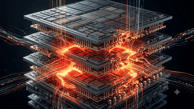
Thermal Simulation Challenges and Solutions in 3DIC AI Chip Design
As AI workloads push chips to deliver ever higher compute density, designers are increasingly turning to three‑dimensional integration (3DIC) to stack dies vertically and pack more functionality into limited footprints. While 3DIC architectures unlock significant performance and bandwidth advantages, they also introduce complex thermal behaviors that are far harder to predict and manage than in traditional 2D layouts.

An Attempt at Compiling a Memory+Compute Fusion Thematic Index – A Dual-Track Framework
Most AI investors talk about “compute” as if it were the whole story: GPUs, accelerators, chips, cores. But every one of those cores needs somewhere to read from and write to. Memory and storage define how wide the data highway really is. In practice, AI performance is a fusion of compute and memory, not a solo act. So why do so many indices and ETFs separate them into different silos—one for semiconductors, one for memory, one for data centers—when the actual workloads keep blending them?
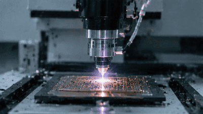
Surging Demand for Laser Drilling and Plasma Dicing Equipment in Advanced Packaging
Advanced packaging has become one of the semiconductor industry’s most important growth engines, and it is now pulling a surprising set of process tools into the spotlight. Among the most in-demand are laser drilling and plasma dicing equipment. These machines sit close to the heart of heterogeneous integration, fan-out packaging, wafer thinning, TSV formation, glass substrate processing, and other advanced flows where precision, yield, and throughput matter enormously. As packaging moves from a back-end afterthought to a strategic platform, the equipment used to shape, open, and separate materials has become just as important as the dies themselves.

D2D Interface Bandwidth and Latency Comparison in Chiplet Architectures
Chiplet architecture has turned the package into a real performance battleground. Once multiple dies are placed side by side or stacked within the same advanced package, the quality of the die-to-die, or D2D, interface becomes one of the most important determinants of system behavior. Bandwidth is no longer a nice-to-have metric, and latency is no longer a small implementation detail. Together, they shape whether a chiplet system feels nearly monolithic or frustratingly fragmented.

Stock Selection Logic and Alpha Validation of ESG-Themed Semi ETFs
Semiconductor themed ETFs are no longer just about growth and cycles. A growing subset now layers environmental, social, and governance (ESG) criteria on top of traditional sector exposure. These ESG semi ETFs promise two things at once: access to one of the market’s most powerful secular themes, and alignment with sustainability and governance standards. The pitch is appealing, but it raises two hard questions. First, how exactly are these stocks being selected? Second, does the ESG overlay help, hurt, or leave alpha unchanged?